显示标签为“PCB”的博文。显示所有博文

2017年11月27日星期一

PCB Background

Printed circuit boards are independent modules of interconnected electronic components, always found in devices ranging from common buzzers, pagers, radios to complex radar and computer systems. The circuit is formed by depositing or printing a thin layer of conductive material on the surface of an insulating board known as the substrate. 
Individual electronic components are placed on the substrate surface and soldered to the interconnected circuitry. The contact fingers along one or more edges of the substrate serve as connectors to other PCBs or external electrical devices like on-off switches. The printed circuit board may have circuitry that performs multiple functions or a single function like a signal amplifier.
Printed circuit board structure has three main types: single-sided, double-sided and multilayer. Single-sided panels have components on one side of the substrate. When components number on a single-sided board is excessive, a double-sided board can be used. Electrical connections between the circuits on each side are made by drilling holes through the substrate at appropriate locations and plating the interior of the holes with a conductive material. The third type, multilayer board, has a substrate composed of a printed circuits separated by insulated layers. The surface components connect to the appropriate circuit layer through plated holes. This greatly simplifies the circuit mode.
Components on a printed circuit board are electrically connected to the circuit in two different ways: through hole technology and surface mount technology. With through-hole technology, each component has thin wires or leads that pass through the holes in the substrate and are soldered to the connection pads on the opposite side. Gravity and friction between leads and hole sides keep the assembly components in place until they are soldered. 
Using surface mount technology, stubby J-shaped or L-shaped legs on each component make direct contact with the printed circuits. A solder paste consisting of glue, flux and solder is applied at the contact points to hold the assembly components in place until the solder melts or reflows in the oven for the final connection. Although surface mount technology requires more attention to component placement, it eliminates the time-consuming drilling process and space-consuming connection pads inherent with through hole technology. Both technologies are in use today. Therefore, it is used more widely than through-hole technology currently.
The other two types of circuit assemblies are related to the printed circuit board. Integrated circuits, also known as ICs or microchips, perform similar functions to printed circuit boards except that integrated circuits have more circuits and components. The hybrid circuit, as its name implies, looks like a printed circuit board but contains some components that grow on the surface of the substrate instead of being placed and soldered on the surface.

2017年1月10日星期二

PCB Design Rules

When you design a printed circuit board, you need to follow the PCB design rules of your manufacturer. These rules are the limits of the machine that makes the circuit boards.
The rules we need to pay attention to are these:
Minimum trace width: The minimum trace width is the minimum width of your traces. So you have to make sure you draw your circuit board “wires” with a width of more than 0.1524 mm.
Minimum trace/ vias/ pads space: Outside each trace, via or pad needs some space. In this case it has to be at least 0.1524 mm. 
Minimum silkscreen width: The silkscreen is what we use to draw or write text on a circuit board. The width of the silkscreen has to be at least 0.1524 mm.
Drilling hole and finish hole: The drilling hole has to be between 0.3 mm and 6.35 mm. And the finish hole between 0.8 mm and 6.35 mm.
SMT minimum solder mask width: This is the minimum width of the solder mask. Solder mask is something that the solder doesn’t like to stick to. So it is around all pads to keep the solder on the pad. And in this case it has to be at least 0.1 mm.
Min solder mask clearance: The solder mask clearance is the space that is needed around the solder mask. 0.13 mm is better.
Learn more about PCB design tips, pls visit www.epcb.com

2016年12月28日星期三

Wave Soldering

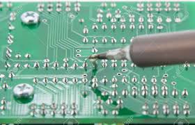
Wave soldering is a bulk soldering process used in the manufacture of printed circuit boards. It is used for both through-hole printed circuit assemblies, and surface mount. However, wave soldering problems is common during a PCB fabrication process
This can be caused by a variety of reasons and the primary one which comes to our mind in the first time is bad plated through-hole barrels. So check the plating in the barrels to make sure there are no voids is very crucial in a wave soldering process. Voids will have a tendency to create outgassing and this creates voids in the solder joints.
The other issue is to bake the boards to expel moisture trapped in a PCB. Great experience in successfully eliminating voids by pre-baking boards and storing them in vacuum sealed bags is really useful. You should know that once a board is baked, if left out in the open air, it will reabsorb 75% of the moisture you just baked out of it within 48 hours. So before wave soldering, make sure the moisture of your board could be as lowest as possible, or you can find voids appeared.
More info. about PCB soldering, pls visit www.epcb.com

2016年12月27日星期二

Disturbed Solder Joint

What is a disturbed solder joint? This is an interesting and difficult question to answer. To simplify, the formation of a disturbed solder joint happens during the solidification process of the alloy. When alloys are in their molten state their surface appearance can be easily affected by outside mechanical influences.
Major cause for the formation of a disturbed solder joint is usually due to some outside vibration of the assembly during the cooling process. Another is easily caused by operators. Reaching into a system and removing an assembly prior to the solder joints ability to solidify, or the PCB transferring from one conveyor to another while the alloy remains in the liquid state. It is the movement of the assembly while the alloy is in the liquid state that creates a disturbed solder joint. 
If you solder a disturbed joint by mistake, it doesn’t matter because the joint can be repaired by reheating and allowing it to cool undisturbed. in addition, you can prevent it by prepare properly which includes immobilizing the joint and stabilizing the work in a vise.
More info. about soldering, welcome to www.epcb.com

2016年12月1日星期四

Salvaging Parts

When you are working on a new project it can be beneficial and economical to find printed circuit boards and components from your old electronic products which can be reuse. This lets you test out your application in the early stages and work on your overall project design before ordering PCBs. Though reusing older parts will cut down on your costs, it may limit the performance of you new products to some extent.
Recycling your old PCBs and designing new advanced ones in their place will help you unlock the potential of your application as it continues in its development.
EPCB dedicates itself to producing the highest quality PCBs and products while minimizing any negative effects that manufacturing can have on the environment. Every piece of scrap PCB boards produced from EPCB’s manufacturing processes is taken directly to a certified refinery to ensure they are responsibly extracted and recycled. 

2016年11月29日星期二

PCB Plating Finish

When you are in the process of designing your PCBs, you have a lot of decisions to make in order to make sure that your finished PCBs can work best for your application. One of these decisions is to choose a suitable printed circuit board plating finish. Although there are multiple plating finishes available, each has its own unique benefits that can either make or break your PCBs. Hot air solder leveling (HASL) keeps fabrication costs low and is excellent for both solder wettability and solder joint integrity. A lead-free HASL finish is also available. In addition, printed circuit boards may be plated using electroless nickel immersion gold, which provides excellent co-planarity, immersion silver, which offers low resistance and high speed, or immersion tin, which is used to create a layer of metal that results in a flat finish. Other options include organic solderable coatings (OSP), and electrolytic nickel gold. Consult a PCB expert to learn about your best option.

For more info. about PCB surface finish, please visit www.epcb.com

PCB Finishes

You may think that the surface finish of your printed circuit board only plays a small role in the cost of your project. However, the finish you choose for your PCB can have significant effects on the quality of your boards.
RoHS finishes for your PCB order vary based on applicability and cost. Four of the most common finishes available include the following:
1.Hot Air Surface Leveling (HASL) – HASL is the least expensive you can buy. This option is a good economical choice for through-hole boards but since they have very low surface planarity, they may not be compatible with all SMT boards.
2.Immersion Tin – Immersion coatings are used to create a layer of metal that results in a flat finish. Tin is the least expensive material you can get using the immersion process, but it may not be ideal because the tin layer begins to tarnish immediately.
3.Immersion Silver – Immersion silver is applied in the same way as tin, but it has a longer shelf life because it does not react with the copper. However, if the PCBs are not stored properly they can begin to oxidize and should be placed and reflowed within 24 hours after removing them from packaging.
4.Electroless Nickel Immersion Gold (ENIG) – ENIG is made up of chemically deposited nickel followed by a layer of immersion gold. This option offers several years of shelf life and has better solderability than both tin and silver.

For more info. about PCBs, please visit www.epcb.com

2016年11月28日星期一

PCB Panelization

PCB panelization, also known as the processing of boards in an array format, keeps small boards attached to each other within a single, larger substrate. As circuit boards become smaller, changes to production processes must be made in order to ensure that quality is not sacrificed. Panelization helps to address these issues to process multiple small boards through assembly, and is becoming more prevalent as board sizes shrink.
There are two primary reasons for using an array scheme: One is to increase throughput, and the other to allow the manufacturing process to maintain its standard panel size. Besides, smaller boards run the risk of being removed during routing due to the router’s vacuum pressure, while the risk can be largely reduced when boards are arrayed in a good order.

For more information, please visit www.epcb.com