2016年12月28日星期三

Wave Soldering

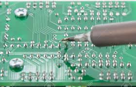
Wave soldering is a bulk soldering process used in the manufacture of printed circuit boards. It is used for both through-hole printed circuit assemblies, and surface mount. However, wave soldering problems is common during a PCB fabrication process. 
This can be caused by a variety of reasons and the primary one which comes to our mind in the first time is bad plated through-hole barrels. So check the plating in the barrels to make sure there are no voids is very crucial in a wave soldering process. Voids will have a tendency to create outgassing and this creates voids in the solder joints.
The other issue is to bake the boards to expel moisture trapped in a PCB. Great experience in successfully eliminating voids by pre-baking boards and storing them in vacuum sealed bags is really useful. You should know that once a board is baked, if left out in the open air, it will reabsorb 75% of the moisture you just baked out of it within 48 hours. So before wave soldering, make sure the moisture of your board could be as lowest as possible, or you can find voids appeared.
More info. about PCB soldering, pls visit www.epcb.com

Solder Bridge

A bridged solder joint is formed by melting two solder joints together, forming an unintended connection between the two. The spacing between connections is quite tight, so you can easily bridge across two terminal connections. You can check by testing for shorts between each connection or use a magnifying glass to visually examine the connections.
You can avoid this only by using enough solder to make a good joint, because solder bridges often happen between joints with too much solder to begin with. If you have to tackle the solder bridge, it is not difficult. Sometimes the excess solder can be drawn off by dragging the tip of a hot iron between the two solder joints. If there is too much solder, a solder sucker or solder wick can help get rid of the excess.
More tips about soldering, welcome to www.epcb.com

2016年12月27日星期二

A Broken Solder Pad

This is a common problem, especially when re-doing wiring. A combination of heat and the physical stress of removing a wire can cause the copper pad to break away from the copper trace leaving a fine gap between the two. The best way to check this is to use a multimeter to check a gap between the pad and the destination of the connection. Follow the trace from where the pad connects to another visible connection point. These can usually be repaired by taking an ink eraser and rubbing down the trace right by the pad to expose base copper and then heating the existed solder and use the iron's tip to drag the molten solder out over the exposed copper of the trace to make the connection. Recheck with the multimeter to validate that you not have a connection from pad to destination of trace. If the gap is significant, use a piece of fine bared wire to bridge the gap and then solder a trace and a joint is a good choice.
To avoid the above problem, you'd better read more about soldering on www.epcb.com

Disturbed Solder Joint

What is a disturbed solder joint? This is an interesting and difficult question to answer. To simplify, the formation of a disturbed solder joint happens during the solidification process of the alloy. When alloys are in their molten state their surface appearance can be easily affected by outside mechanical influences.
Major cause for the formation of a disturbed solder joint is usually due to some outside vibration of the assembly during the cooling process. Another is easily caused by operators. Reaching into a system and removing an assembly prior to the solder joints ability to solidify, or the PCB transferring from one conveyor to another while the alloy remains in the liquid state. It is the movement of the assembly while the alloy is in the liquid state that creates a disturbed solder joint. 
If you solder a disturbed joint by mistake, it doesn’t matter because the joint can be repaired by reheating and allowing it to cool undisturbed. in addition, you can prevent it by prepare properly which includes immobilizing the joint and stabilizing the work in a vise.
More info. about soldering, welcome to www.epcb.com

2016年12月26日星期一

Insufficient Wetting

Wetting is the ability of a liquid to maintain contact with a solid surface, resulting from intermolecular interactions when the two are brought together. The degree of wetting (wettability) is determined by a force balance between adhesive and cohesive forces. Wetting is important in the bonding or adherence of two materials. So what’s the result of insufficient wetting? Here EPCB lists 3 examples. 
Insufficient Wetting (Pad): Suppose a solder has wetted leads nicely, but it has not formed a good bond with the pad. This can be caused by a dirty circuit board. 
Insufficient Wetting (Pin): If a solder in a joint has not wetted the pin at all and has only partially wetted the pad. In this case, heat was not applied to the pin and the solder was not given adequate time to flow.
Insufficient Wetting (Surface Mount): Assume that we have three pins of a surface mount component where the solder has not flowed onto the solder pad. We can heat the solder pad with the tip of the iron, then apply solder until it flows and melts together with the solder already on the pin.
More info. about printed circuit board soldering, welcome to www.epcb.com

Cold Solder Joint

Cold solder means the solder is more or less in the right place, but isn't actually bonded to one or more of the metal surfaces in the joint, so the solder bond will be poor and the cracks may develop in the joint over time. A cold joint is one where the solder did not melt completely. Thus, it is unreliable and often characterized by a rough or lumpy surface. It can also happen when you're soldering materials that haven't been prepared for soldering. For example, bare aluminum is a real pain to solder.
To prevent cold joints, make sure every surface you want to solder is actually being heated to the melting point of the solder. If you're using a soldering iron, it should touch every metal surface in the joint. Don't use the iron to melt the solder. Wait for the heated surfaces to melt it. 
If you still find cold solder joints on you circuit board, don’t worry. They can usually be repaired by simply re-heating the joint with a hot iron until the solder flows. Many cold joints also suffer from too much solder. The excess solder can usually be drawn-off with the tip of the iron.
More info. about solder, pls visit www.epcb.com

2016年12月25日星期日

E-Waste

E-waste or electronic waste is the left over PCBs, components, PVC or plastic cases, body, etc., of your old electronic appliances, such as a TV, refrigerator, dish washer that you have thrown out. It is one of the fastest growing types of waste produced on the planet. According to a report on e-waste, by 2017, all of that year’s end-of-life refrigerators, TVs, mobile phones, computers, monitors, e-toys and other products with a battery or electrical cord worldwide could fill a line of 40-ton trucks end-to-end on a highway straddling three quarters of the Equator, the weight equivalent of 200 Empire State Buildings or 11 Great Pyramids of Giza. The US has the world’s highest figure of 9.4 million tons and China generated the second highest e-waste total of 7.3 million tons. The report also states that the total amount of e-waste generated by 2017 will be 65.4 million metric tons.
What can we do to stop the severe situation? Well, the simple answer is stop over-consumption. But that could take a long time to actually come into action. The next big thing is too start recycling every bit of those electronic appliances and gadgets that our leaving our house. We can open up the body of each of these appliances take out the PCBs and reuse the components.
Learn how to reuse printed circuit boards, welcome to www.epcb.com